


Wafer inspection: yellow LED lighting system for high-quality wafer testing
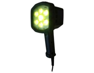
Yellow Wafer Semiconductor Inspection Lamps from SECU-CHEK
(Wafer Semicondutor Inspection Lamps SLEX-GB-H127-SFN-DNF)


Optical wafer inspection specially designed for quality assurance and testing of wafers
integration of the systems into existing reactors
Wafer surface inspection to increase ROI
Wafer inspection with yellowlight lamps / wafer surface inspection with greenlight lamps
- Wafer inspection with High-Tec yellow light lamp without UV radiation
- Replacement of UV lamps for inspection of wafers
- Testing of wafers without the use of mercury vapor lamps
- Designed as a filtered green light lamp or as a filtered yellow light lamp for wafer inspection
- Wafer surface inspection with SECU-CHEK wafer test lamps without UV and without mercury
Choose a robust, low-maintenance yellow light lamp for optical wafer inspection
with comprehensive process reliability thanks to extremely strong display of failures
and enormous energy savings compared to 100 watt mercury discharge bulbs


Why use filtered Yellow Light Lamps from SECU-CHEK for Wafer Surface Inspection?
- High process reliability required for wafer production
- economically efficient and trouble-free test operation desired
- solid wafer testing is critical to the further cost-intensive steps of wafer preparation and chip production
- Professional solution according to industry standard required
Request now price for the wafer Semicondutor Inspection Lamp SLEX-GB-H127-SFN-DNF from SECU-CHEK!


What are the errors in wafer production and how well are they recognizable with the SECU-CHEK yellow light lamp?
- Faults of the wafer are well detectable with the filtered yellow light lamp
- Detect inclusions with the wafer test
- Detect contaminations by visual wafer testing
- See growth disturbances with yellow-green light
- Identify veils during optical wafer test
- Analyze stripes with the SECU-CHEK wafer inspection lamp
- Detect microstructures better compared to UV lamps and mercury lamps for wafer testing
- Detect growth holes with wafer inspection
- Check the edge flattening with high contrast of the yellow-green lamp
- Edge interferences can be found with the optical wafer inspection
- Detect structural shifts with the quality inspector lamp on the wafer
- Detect inclusions in wafer production with UV yellow light and green light lamps
- Idendify unevenness with the filtered yellow light light
- Identify limited clarity through high-quality wafer inspection
Common questions when visually inspecting wafers with yellow light lamps
- What illumination and intensity do I need for reliable test results during wafer inspection?
- Where/How are the lamps integrated for surface testing of the wafers in order to enable efficient workflows?
- What are the mounting options and open spaces for the yellow light lamp in the laboratory area?
- Do the processes and safety mechanisms of the yellow light or green light lamp meet the requirements that we have to meet?
- Who takes care of the instruction for error detection during the wafer test?
- What maintenance and repair costs do I have to plan for the UV lamp for wafer testing?
The yellow light lamps and green light lamps from SECU-CHEK with the special LED technology enable you to offer a solution that is perfectly adapted to your test situation. Request a yellow light lamp to test your wafers today!

Wafer Inspection Technology for Chip Manufacturing and Solar Manufacturing
Manual wafer testing with high-tech yellow light lamps
- strong, extremely uniform, low-shadow illumination at the required intensity
- many advantages over automated wafer inspection – reduce the reject rate
- optimal for visual post-inspection of sorted wafers during automatic wafer inspection
- Evaluation and testing of all types of wafers in wafer production
 Manual optical wafer testing
- Easy integration of visual inspection into the wafer manufacturing process
- all kinds of wafers in photovoltaics as well as silicon wafers and much more. More
- High flexibility in wafer inspection with high error detection rate
Yellow filter and green filter for perfect visual inspection
- robust yellow light lamp housing for continuous operation during wafer inspection
- easily replaceable filter disc for the wafer lamp
- UV wafer lamp optional with active fan cooling for particularly long service life
Improve wafer production with manual wafer inspection
- Yellow light lamp for wafer testing: emitted in an optimized wavelength range, including the wavelength of 546, 577 and 579 nm, typically emitted by inspection lamps based on mercury vapour discharge bulbs as peak wavelength
- yellow better than green (525 nm) for high-contrast detection
- no flickering during the wafer test
- dimmable yellow light lamp that can be used to adjust the intensity to the best level for all types of inspections and types of errors
- Inspection lamp for semiconductor wafers
- LED-based replacement for common yellow light lamps
Which types of wafers can be tested with the SECU-CHEK yellow light lamp?
 Wafer inspection in semiconductor and chip manufacturing
- Wafer testing for the solar industry and photovoltaics
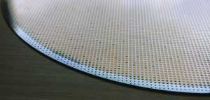
- visual wafer surface testing for all wafer sizes: 25mm (1-inch), 38mm (1.5-inch), 51mm (2-inch), 75mm (3-inch), 100mm (4-inch), 125mm (5-inch), 150mm (6-inch), 200mm (8-inch), 300mm (12-inch), 450mm (18-inch)
- Inspection of epitaxed wafers
- optical testing of monocrystalline wafers and also polycrystalline wafers
- visual test of the surface of silicon wafers
- Check also possible for square wafers
- Testing of raw wafers and structured wafers
- Analysis of the surface of epitaxy wafers (EPI wafers) and SOI wafers
- Gold wafers test with the yellow light lamp
- Visual inspection with the UV lamp for crystalline silicone wafers
- Optical surface inspection for wafers of all materials: silicon, germanium, slicium carbide, gallium arsenide, sapphire, glass, etc.
- Visual inspection for SEMI standard wafers
- Quality check of bonded wafers, wafers on tape
- visual wafer inspection also for bare, thinned and fan-out wafers
- Optical quality control and inspection of strongly curved wafers (eLWB, etc.)
- etc.
 Wafer inspection in semiconductor and chip manufacturing
Particle Detection and quality control to reduce contamination in wafer production / semiconductor production
In addition to the visual surface inspection during wafer inspection, in which wafer inspection is carried out by means of a yellow light lamp or green light lamp, partly automated, many semiconductor manufacturers have further requirements:
- Use test lamps to check for particle contamination in the systems
- Particledetection with yellow light lamps or with UV-LED lamps
- Particle search for quality control in the cleanroom during wafer production
- Search and find particles for cleaning the machines in semiconductor production
- Cleaning and keeping clean production equipment in the course of continuous quality control
Contamination of production facilities is a critical factor for smooth production and thus business success. In most cases, the particle detection can only be carried out with manual inspection and thus with mobile yellow light lamps, green light lamps or UV LED lamps.
Let us advise you on how to seamlessly and effectively integrate optimal quality control into your existing wafer production processes with SECU-CHEK’s leading wafer inspection technology.
We look forward to your inquiry!
You are also welcome to contact us by phone or email.
Direct contact:
SECU-CHEK GmbH
An der Fähre 9
66271 Kleinblittersdorf
GERMANY
Phone +49 6805-942859-0
Fax +49 6805-942859-95
Email: info@secu-chek.de

By loading the map, you agree to Google's privacy policy.
Learn more
Wafer manufacturing - Knowledge and information
What is a wafer?
- Wafer stands for “thin biscuit” or “thin slice”
- a wafer is mostly circular, but partly also square
- the production of wafers is carried out from so-called ingots
- Wafers are usually a base plate for electronic components and elements
Use of wafers
- Chip production (integrated circuits)
- Microelectronics
- Photovoltaic (solar cells)
- Microsystem technology
More interesting information about wafer production and inspection
- Optical inspection solutions for highly integrated wafer testers
- Wafer inspection
- Inspection system for silicon wafers
- Automated wafer inspection
- Semiconductor Wafer Inspection
- Fully automated wafer inspection – YouTube
- Optical Wafer Inspection
- New measurement method for wafer inspection (article in german language)
Building a wafer
- Material: mostly silicon, partly also silicon carbide, gallium arsenide and indium phosphide
- partly also glass or gold wafers
- Size: 1 inch wafer to 18-inch wafer, with 18-inch wafers not yet possible for mass production
- there are various methods for the production of the ingots, e.B. the Czochralski process, etc.
Wafers in photovoltaics
- Differentiation of polycrystalline (multicrystalline) and monocrystalline wafers
- Wafers are produced by sawing the ingots
- square-shaped silicon blocks mostly for solar cell production
- round, monocrystalline wafers of cylindrical ingots mostly for chip manufacturing and microelectronics
More information about wafer production, wafer testing, etc. can be found here: Wikipedia